A PHY for All Seasons: MIPI M-PHY Takes Center Stage
About the Authors:
Ashraf Takla
President & CEO, Mixel, Inc.
George Brocklehurst
Marketing Director, Nanotech Semiconductor
The curtain is up and the M-PHY® specification is taking center stage, positioned to handle the many different roles required for a faster, more reliable, physical interface layer (PHY Layer) on mobile devices. The script for the M-PHY specification was written inside the MIPI® (Mobile Industry Processor Interface) Alliance by a working group made up of member companies and set up to expand the capabilities of mobile devices by defining interface standards that will revolutionize the capabilities of the coming generations of mobile products. Anchored in the PC world, “standards” like PCI Express and DisplayPort have not crossed over, nor become accepted in mobile devices. Because of the aggressive power targets set by the mobile industry for the Physical Layer (PHY), these PC standards were not reusable in the mobile space. Now faced with an explosion of mobile multi-media devices with an ever-increasing demand for faster throughput, the mobile industry, through the MIPI Alliance, has defined the ultimate PHY, one capable enough to handle the demands of mobile devices and seems capable of moving into several other key application areas as the PHY of choice.
Mobile Mania
The mobile market is exploding with device after device, from smart phones to e-readers. These portable products are impacting almost everyone—every day. A total of 1.2 billion mobile-phones were shipped globally in 2009, and the expectation is that this number will nearly double to 2.25 billion by 2014. The announcements of new products also continue. The introduction of Apple’s new iPad is just another example of the excitement around this market. Because the portable consumer market is driven by keeping costs and power low, while improving function, controlling cost is critical to the overall success of a product. The wrong mix of cost and function, elevating the price, creates a product that can languish, producing only limited sales, never reaching its full market potential. The development of “Industry Standards” (Standards) is important in controlling costs. Standards guarantee interoperability allowing companies to independently accelerate development, while giving systems integrators multiple supplier options.
MIPI and the M-PHY
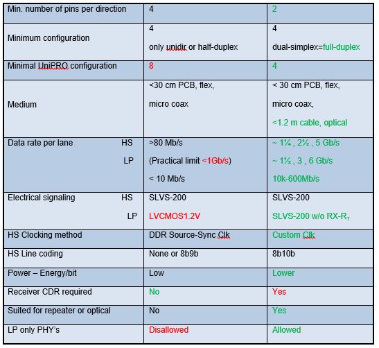
The M-PHY specification is an essential part of the MIPI Alliance’s vision for new and more capable high-speed interfaces on mobile devices. Members identified early the need for a serial interface to support the ever-increasing data bandwidth requirements of mobile devices. Now, pressed even further by the explosion of digital content in video, social media exchanges, and cloud computing, mobile devices require a faster physical layer interface, like the M-PHY, to remain a step ahead of the data transfer requirements necessary to give consumers the on-device response they need. Fuelled by the success of the other MIPI Standards now being deployed; the M-PHY specification is gaining momentum as it moves toward final approval as the newest MIPI specification. The MIPI D-PHY, a source synchronous interface that is currently handling the interfaces between the application processor chip and the camera or display in a mobile device, has been especially successful. Even though the D-PHY is a capable interface, its synchronous nature has speed limitations (1 Gigabit per second) that prevent it from handling the demands for higher data transfer rates. The industry requires a more powerful PHY, one that offers asynchronous data transmission and addresses the speed and signal integrity issues of high-speed chip-to-chip connections within an increasingly EMI (Electro-Magnetic Interference) sensitive environment compounded by tighter form factors, while continuing to minimize power dissipation. The M-PHY specification, slated to handle these high-speed issues, is becoming a silicon reality.
M-PHY Use Model
A “Use Model” is a description of whom, where and how a described capability will be used in a product or application. Defining a Use Model for any new Standard is critical, because without a real understanding of how a Standard will be used, it will never deploy effectively.
Since the MIPI Alliance member companies, who span the entire cell phone value chain, are committed to a successful Standards definition process and eventual deployment, such a Use Model was in place early, and continues to be used to focus decisions in the specification details. Member companies have defined Use Model cases that form the basis of the required feature set.
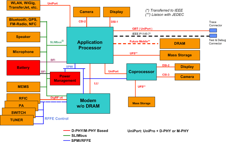
Members like Motorola, Nokia, Intel, Samsung, ST Ericsson and Texas Instruments, have been at the forefront of defining these usage models. Input comes from a breadth of companies, Systems-OEMs to semiconductor and Intellectual Property (IP) providers. A specification is developing that offers a wide range of transfer frequencies and data transfer mechanisms. Many Use Model representations for the M-PHY specification follow a pattern similar to the diagram in Figure 1.
The Stage and Script
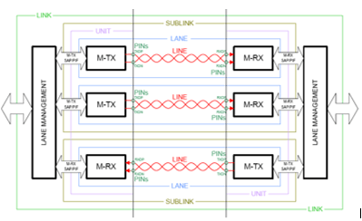
The basic architecture of an M-PHY system is shown in Figure 3. Each LINK is made up of two SUBLINKs, containing one or more LANEs. A LANE is a unidirectional point-to-point differential serial connection between PINs, called a LINE, and connects an M-PHY transmitter and an M-PHY receiver. LANEs running in the same direction constitute a SUBLINK. Two SUBLINKs running in opposite directions, plus the additional management function, complete a LINK. Thus, the operation of the M-PHY interface is completely defined in the context of a protocol definition like DSI, CSI, UniPro, or DigRF which manage the LANE.
There are two fundamentally different types of M-PHY interfaces, denoted as Type-I and Type-II, depending on which signalling scheme is used. For low-speed operation, Type-I employs PWM (pulse width modulation) signalling, while a Type-II uses system-clock synchronous NRZ (non-return-to-zero) signalling. Type-II requires a shared reference clock between the two ends of the line. Type-I is able to operate with independent local clock references on each side of the link. Type-I and Type-II are not interoperable, but implementations may support both types of in order to enable hardware reuse, so that one M-PHY specification can service multiple applications and connections inside a mobile device.
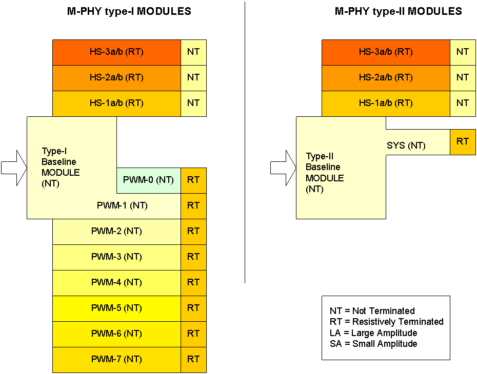
The two modes are illustrated in Figure 4. For PWM signalling (Type-I), there are multiple GEARs (they can switch like gears in a transmission) to cover different speed ranges. The default (mandatory) GEAR for Type-I is PWM-G1, ranging from 3 to 9 Mbps. There are six GEARs with incremental 2x higher speed ranges (PWM-G2 to G7), and one GEAR below the default speed range (PWM-G0). This GEAR-based architecture and the modulation scheme enable an M-PHY specification to optimally target data rates and power dissipation based on system requirements. The M-PHY interface can optionally support a high-speed mode (HS-MODE). The HS-MODE includes a default GEAR (HS-G1) and two optional GEARs (HS-G2 and HS-G3) at incremental 2x higher rates. For any given supported HS GEAR, all lower HS GEARs must always be supported e.g. support for HS-G3 alone is not allowed. Each GEAR includes two baud rates for EMI mitigation reasons, e.g. HS-G1 supports 1.25Gbps and 1.45Gbps. This is especially useful for supporting one handset sold in two geographical regions, which have different base-band frequencies; if one region with a particular base-band frequency suffers beating interference from PHY EMI the alternate rate may be selected. The G2 and G3 GEARS would operate at 2.5Gbps and 5Gbps respectively. Type-II uses a shared reference clock and thus does not require clock recovery. Between the architecture and the clocking options, the M-PHY specification enables the construction of a very versatile set of PHY operations that can target many different LINK requirements. The M-PHY definition is a complete “script”, in specification form, ready for “staging”, in silicon, and capable of handling the speed and power requirements of the next generation of mobile devices.
An Award-Winning Role
The versatility of the M-PHY interface can be seen in how well it fits into systems defined in the Use Models by those MIPI members that need it to play many different parts. The impressive qualities of the M-PHY interface demonstrate why it will be an industry hit upon deployment. One upcoming role for the M-PHY is addressing next generation camera application requirements, which the D-PHY will be hard pressed to meet. Looking at the graphs below, you can see how ever increasing camera resolution will drive the demand for higher data rate requirements that can only be handled effectively by using the M-PHY interface. The first graph, Figure 5, shows the evolution of higher pixel resolution over time.
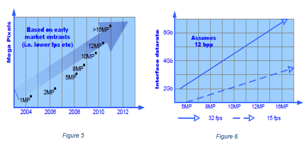
High-speed data rates are required to support the viewing of digital media from still and video capture. Digital photo media are constructed from many pixels, each pixel with a unique value representing its color depth (represented in bpp or bits per pixel). As the camera resolution on mobile devices improves, the files that result from still or video capture become larger and larger. These images need to be stored or moved across a mobile device.
Figure 6 shows the required interface rates as a function of the Mega Pixels (MP). The throughput requirements for two different frame refresh rates (32fps and 15fps-frames per second) are plotted. At 12 bits bpp, 4096 colors are supported, and the files sizes increase such that at 12MP the required interface data rate is close to 6Gbps. The reason that 12 bit color depth is used is that it represents a minimum limit for high quality digital photos displayed on mobile devices such as PDA’s and phones. Less than 12 bits distorts the digital photo colors too much. The color depth to reach a proper viewing experience is balanced against the bpp number (12) since the lower the bpp number, the less memory and resources are needed. To achieve 6Gbps bandwidth the M-PHY interface is the only logical choice.
Working the Media
The motivation for specifying a more capable PHY not only has to do with adding exciting new features, but also with improving the reliability of mobile devices. Connecting two sides of a clamshell phone, requires interconnect flexible enough to withstand mechanical stressors, at transfer speeds high enough to satisfy the applications requirements, and signal quality good enough to ensure reliable reception. In addition, this PHY must dissipate minimal power and contribute little EMI. The connector medium used has historically been thin (< ~1 mm) copper wiring. As few wires as possible should cross the connection so that signal integrity problems remain in check without constraining the handset design, hence the strong preference for high speed serial interface.
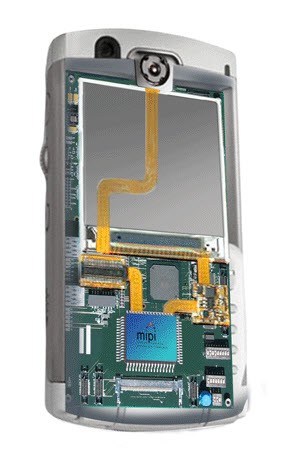
Optical links offer a robustness and mechanical flexibility, along with superior EMI and noise immunity. Some mobile devices have complex hinge (flip-side-twist) mechanicals. These hinges give viewers control over their view angle, which is very important when the display is smaller, and when it’s necessary to reduce eye and neck stress. One example of a complex two axis movement is shown in Figure 7, where the first access acts like a flip phone and the second allows adjustment of the display viewing angle. The data rates across these hinges and the susceptibility to mechanical failure limits the number of copper connections that cross the hinge and the materials that can be used to maintain reliability.
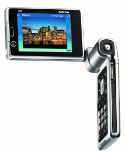
Advanced mobile devices have axis movements that add mechanical stress to interconnects between the display and processor/ Source: Nokia Corporation
Optical interconnect allows the rules to be re-written and decouples system architectures from handset form-factor design, allowing a common platform to be used across many handset models regardless of hinges, features, and physical attributes.
Traditionally the optical components have been viewed as overhead in terms of power and cost, and to a large extent this is true, since portable consumer electronics cannot tolerate an extra couple of dollars on the BOM or some additional milliwatts. However with serialization and the resulting increase in data rates, copper solutions become comparable in cost (@ ~3Gbps) and don’t offer the ancillary benefits of optical. Furthermore optical offers improvement in the $/Gbps and mW/Gbps ratios as the data rate goes up offering a forward looking roadmap where copper would likely follow a restrictive trend. Add to this the impact that a small fraction of the large consumer volume will have on the cost models within the optical PHY industry, which currently operates on relatively low volumes by comparison, and you will likely see accelerated optical module price reduction and improved performance.
The MIPI PHY Working Group anticipated using an optical medium to mitigate these growing issues, setting up an Optical Sub-Group to define an Optical Media Converter (OMC), that converts electrical signals from an M-PHY Transmit (M-TX) into optical signals (light waves), transports the signals across a medium such as a Plastic Optical Fiber (POF), and converts the optical signals back into electrical signals that an M-PHY Receiver (M-RX) can receive. An OMC is considered to be like a “module”, an inseparable unit, consisting of an optical transmitter (O-TX), an optical receiver (O-RX), each with appropriate photonics, and an optical wave guide. Since OMC is one unit, interoperability between optical modules is not required, and thus the optical domain is not specified within MIPI.
These “modules” are well understood in the high-speed optical markets like SONET/SDH and as part of the IEEE Ethernet, Fiber Channel, and OIF-CEI specifications. The module and its electrical connections are illustrated in Figure 8.

Furthermore, if these high-end video capture and display applications, and the subsystems that support them, dissipate more power, resulting in intolerable ground shifts across traditional copper interconnect, then optical interconnect is even more desirable.
Whether copper or optical fibre is used, the M-PHY specification defines a flexible architecture that allows the implementer to support high data rates at minimal power and cost.The challenging aspects of delivering high-definition streaming video; loading of gigabyte wide movies (from the Internet) in an “everyone, everywhere, seamless wireless connection to surrounding devices and services” will only come from an optimized chip-to-chip interface– like the M-PHY.
The Final Act
The final necessary ingredient for the successful deployment of the M-PHY specifications is a healthy ecosystem of companies that can develop, test, demonstrate interoperability, and deliver the M-PHY infrastructure to market. The collaboration between suppliers who can fill these roles is the final act in realizing the ultimate benefit of all the work done by so many contributors in the MIPI Alliance. One of the key components of a vibrant ecosystem, are the IP providers that can build and deliver the M-PHY subsystem so that rapid adoption can take place. The very nature that makes the M-PHY interface unique, namely its versatility, its many architectural options and its ability to address many different applications, makes a one-size-fits-all IP approach a self-defeating proposition. This is different from other standards such as PCI Express, SATA, or DDR, where a single architecture can be ported to many process nodes to effectively address the requirements of thousands of customers. For the M-PHY to fulfill its potential of being an optimized solution for applications where power, area, and total cost are all parameters of paramount importance, a cookie-cutter approach will not do. Successful MIPI adopters will be those who can partner with an M-PHY IP vendor that can provide a shrink-wrapped, silicon-proven yet customizable, high quality differntiated IP at reasonable cost.
Mixel Inc. has already announced one of its M-PHY customers, Graphin CO. LTD. of Japan. Together the two companies plan to support the MIPI M-PHY ecosystem by building a “Golden M-PHY” IC to be used in Graphin’s evaluation systems. The same “Golden M-PHY” IC will be made available to support M-PHY interoperability and testing requirement of the MIPI ecosystem. Mixel is also collaborating with Nanotech Semiconductor, of the UK, which chairs the Optical M-PHY subgroup, to support the MIPI M-PHY optical ecosystem. Mixel employs what it dubs a “Legorithmic” approach, which enables it to effectively develop efficient, shrink-wrapped MIPI IP, based on its silicon-proven building blocks to meet the large set of M-PHY flavors that will be required for the variety of M-PHY applications.
Every mobile device, every bandwidth hungry new application developed to run on them, and every new capability that pushes the limits of performance, indicate it is time to introduce a PHY to meet these challenges. The curtain is up and the M-PHY is ready to go—a PHY for all seasons.
To learn more about Mixel’s silicon-proven IP, please visit mixel.com/ip-cores or Mixel’s contact page.