MIPI in FPGAs for Mobile-Influenced Devices
About the Authors:
Yundong Cui
Technical Support Director, Hercules Microelectronics
Mahmoud ElBanna
General Manager, Mixel-Egypt
A new wave of applications for mobile-influenced devices, using technology initially designed for mobile devices, demand high-resolution, high-frame-rate streaming data from vision sensors, especially with the rise of AI inference models performing real-time scene and object classification. These applications include automotive, home automation displays, medical device displays, surveillance and IoT sensors, and more. A natural choice for these designs is vision sensor chips with MIPI® interfaces, which help balance performance with power consumption.
Designers may be able to locate and specify an off-the-shelf vision sensor chip with MIPI that fits their mobile-influenced device requirements. However, a significant decision looms if no off-the-shelf chip meets the needs. Many of these applications require customization to fit in devices with reduced size and power, suggesting the design of a custom system-on-chip. Opportunities in this mobile-influenced space typically present smaller unit volumes, making investments in system-on-chip (SoC) implementations harder to justify with SoC design and fabrication costs rising.
The answer to this conundrum may lie in FPGAs — not huge, power-hungry FPGAs that get most of the attention today, but smaller, more power-efficient FPGAs designed with mobile-influenced devices in mind. These FPGAs offer enough performance for MIPI interfaces running in high-speed or low-power states while leaving room for additional customer-supplied logic in a relatively small package. This article explores conditions where FPGAs are a solid design choice, what implementation of MIPI in FPGAs looks like, and some use cases for designers.
Small, low-power FPGAs filling more roles
Advances in semiconductor processes have made FPGA-hosted logic much faster than earlier generations of the technology. FPGA vendors initially targeted these faster devices toward implementations of wired connectivity in server-class platforms around interfaces like high-speed Ethernet and PCIe. Performance and port density are the primary design criteria in rack–mounted data center applications, with power and cooling of some concern but less constrained than in smaller devices.
This faster FPGA-hosted logic is more than fast enough for MIPI interfaces. If there were an FPGA that was fast enough for MIPI and consumed less power in a smaller footprint, mobile-influenced device designers would gain the flexibility to address scenarios where FPGAs play crucial roles.
- Rapid prototyping before committing to SoC development. The market viability of a newly conceived device may rest on delivering a proof of concept (PoC) quickly to secure funding, place on a short-list for a competitive proposal, or obtain customer feedback. The best path to rapid prototyping is an FPGA, where designs can initiate and iterate quickly.
- Low-rate initial production or planned product evolution. Winning the first client opportunity can lead to producing an FPGA-based, production-quality product but in low unit volumes while other customer engagements develop. Another powerful strategy is introducing a minimum-viable product with pre-planned enhancements on a roadmap executed quickly with FPGA logic upgrades.
- Low-volume applications in automation, medical, test equipment, and other niches. Some product opportunities represent thousands of units instead of millions or billions. These low-volume applications often draw the attention of commercial off-the-shelf vendors of boards and systems. However, off-the-shelf products can be challenging to customize; for example, add-on modules expand capability but increase the size, power, and cost. An FPGA-based design gives teams more control of size, customization, and differentiation up to mid-range unit volumes.
- Single hardware version with reconfigurability. Markets worldwide can differ in specific requirements, and producing hardware variants in unique SKUs to target regions gets complicated and costly. An FPGA-based design may meet many regional requirements from a single hardware version, with the FPGA reconfigured for shipment in each region. This approach also simplifies supply chain management and reduces product lifecycle costs.
Since MIPI applications originated in mobile devices, designers may not have had a reason to revisit FPGAs for MIPI interfaces. If designers look now, a new alternative is emerging.
Implementing MIPI in FPGAs
These scenarios are precisely the ones Hercules Microelectronics, a Mixel customer, enables with a MIPI implementation in two low-power FPGA families: the first-generation HME-H1D03 and the second-generation HME-H3C08.
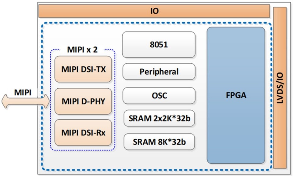
The HME-H1D03 features 2K LUT6 blocks running at up to 200 MHz, along with an integrated, enhanced single-cycle 8051 core, SRAM and peripheral blocks, and two hardened MIPI groups, each with a 1.5 Gbps MIPI D-PHYTM and MIPI DSI-2® Tx and MIPI DSI-2 Rx controllers. Both MIPI groups are configurable for Tx or Rx. Display support is up to 2K resolution (2560×1440).
HME-H1D03 Block Diagram with Mixel MIPI D-PHY

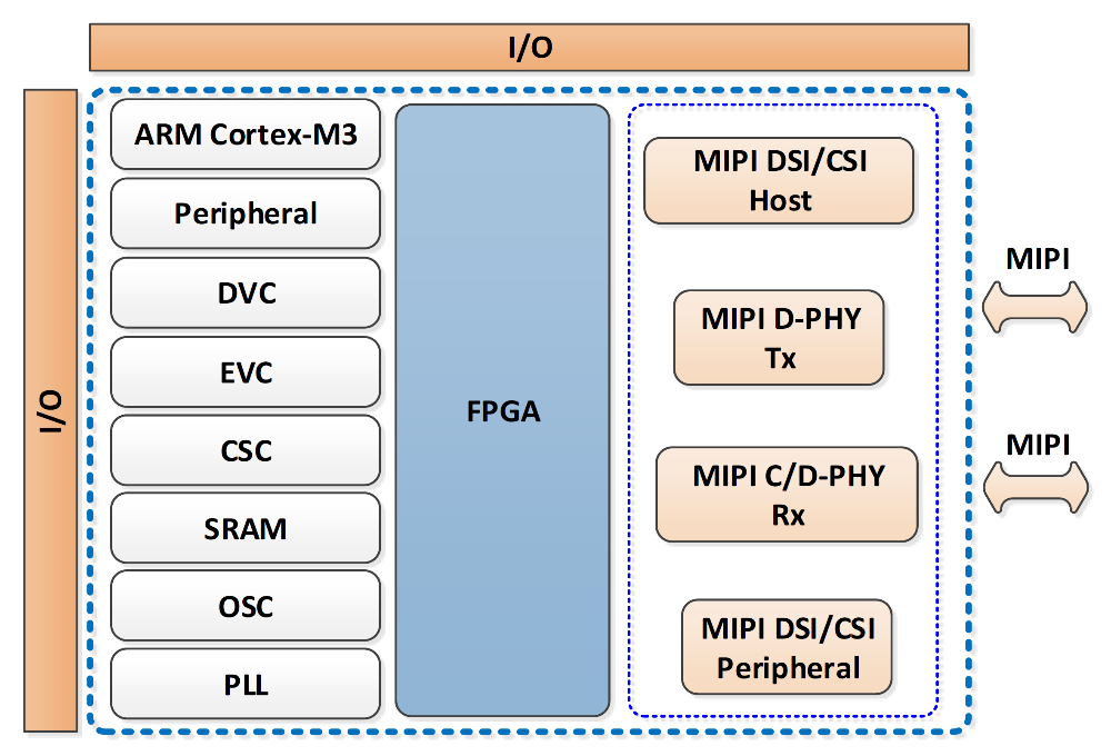
The HME-H3C08 incorporates an ARM Cortex-M3 core, more than doubles its LUT6 blocks to 4992, and increases the speed of the two hardened 4-lane MIPI blocks to 2.5 Gbps. It also offers a broader choice of MIPI IP for more configuration flexibility: MIPI D-PHY and MIPI C-PHYTM as a MIPI C-PHY/D-PHY combo Rx with DSI-2 peripheral and CSI-2® Rx controllers and a MIPI D-PHY Tx with DSI-2 host and CSI-2 Tx controller cores.
HME H3C08 with Mixel MIPI C-PHY/D-PHY Combo and MIPI D-PHY

Hardening the MIPI logic in the FPGA delivers proven Mixel MIPI IP product implementations, saves power through optimization, and leaves a substantial FPGA logic block free for designer use. Instead of dealing with RTL for a MIPI block and taking up valuable LUTs in the programmable logic, designers move directly to configuring the hardened MIPI interfaces and customizing application-specific logic for processing streaming data for their device requirements. The result is a faster mobile-influenced device design cycle, retaining the flexibility needed for differentiating a product.
Mixel’s MIPI IP products offer MIPI specification-compliant configurability for achieving various architectural goals. Two examples are bridging and low-power modes.
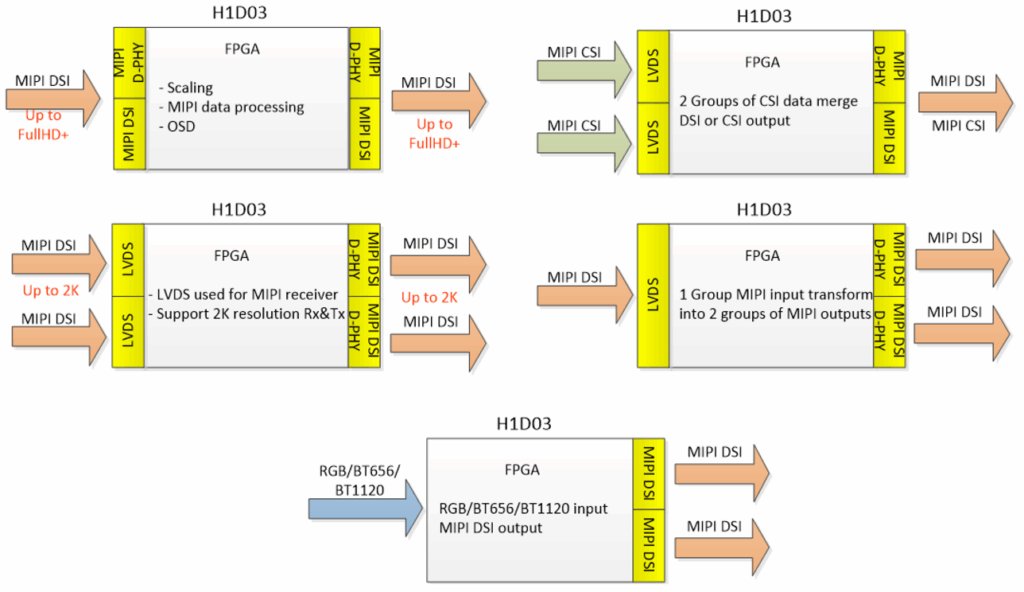
MIPI bridging is a broad term describing the capability to aggregate, split, and post-process MIPI CSI-2 and MIPI DSI-2 signals. The goal is to enable application processors — or an FPGA — to interact with a broader range of displays and sensors, including dual-display or dual-sensor configurations. The two-block MIPI feature opens bridging possibilities like the ones shown next.
H1D03 Low-power FPGA MIPI Use Cases

MIPI interfaces can run in either high-speed mode, providing full display resolution and frame rates, or low-power modes, with reduced data transfer rates saving power. Coordinating sensor resolution and sampling, frame rate, and MIPI transfer rate, with fast switching between modes under application processor control, can balance full-out streaming performance with energy conservation at lower resolution and frame rate when appropriate. Mobile-influenced devices designed around these FPGAs can creatively apply dynamic frame rate control for significant power savings, keeping the sensor chain in low-power mode for prolonged durations until higher performance is needed.
Use cases for MIPI in FPGAs
Incorporating MIPI into low-power FPGAs opens numerous application use cases for mobile-influenced devices. Hercules Microelectronics and Mixel describe six possibilities for various configurations.
- Higher-end display support with bridging. Supporting a 2K resolution display would typically require a high-end application processor. The FPGA can offload a low-end application processor using MIPI bridging, providing up-scaling functions to achieve full resolution.
- Left-right display for AR glasses. Micro LED displays, such as those in eyeglass-frame AR glasses, use a QSPI interface to reduce pin count and package size. The FPGA can receive RGB data over its MIPI interface, split the stream into left-right components, and drive QSPI-connected micro LEDs. The FPGA’s small package size, 4.0 x 4.6 mm for the H1D03 and 4.2 x 4.2 mm for the H3C08, and low power consumption allow an on-frame fit.
- ePaper displays. Unique signaling and timing requirements mean most application processors aren’t designed to drive ePaper displays directly. Again, the FPGA can offload format conversion tasks from an application processor and, with its microcontroller core, can support visual enhancements such as dithering and color mapping algorithms.
- Smart home control panels. Most smart home control panels don’t feature high-resolution, high-frame rate displays. However, they typically require more peripheral integration, which is an ideal use case for FPGA logic. Designers can add Wi-Fi, SD Card, RS-232/485, SPI/I2C touchscreen, and other peripheral support and perform GUI framework processing in the FPGA, operating stand-alone without an application processor.
- Industrial cameras. Sophisticated, single- or multi-spectral sensors for industrial cameras often use LVDS interfaces designed before MIPI’s debut. An ASIC or board-level implementation of a control platform in the camera converts the LVDS stream into a standard connectivity interface, usually Ethernet or USB. This scheme can leave camera makers with a problem if they want to upgrade to a new sensor with a MIPI CSI-2 streaming interface, forcing a corresponding revamp of the control platform design. An FPGA can bring a MIPI CSI-2 stream back to LVDS, allowing a sensor upgrade while preserving the control platform functionality. The FPGA can also perform other pre-processing, such as video data reassembly.
- Dual displays with main and secondary. A more advanced take on the left-right display is a dual-display targeting foldable devices, where a secondary display is on the outer housing when folded, and a full-resolution main display is inside the fold.
H3C08 Low-power FPGA in Dual Display Use Case

These are just some examples where the new-found flexibility of MIPI in FPGAs provides innovative opportunities for the design of mobile-influenced devices. As sensors continue to swing from LVDS interfaces to MIPI CSI-2 and MIPI DSI-2 interfaces, the Hercules Microelectronics HME-H3C08 and HME-H1D03 and other MIPI-enabled FPGA solutions like it should win more opportunities. The scenarios of rapid proof-of-concept, low-volume economic viability, and reconfigurable hardware relieve designers of the burden, risk, and cost of complex SoC design and the challenge of recouping development costs through product revenue. Mixel’s state-of-the-art MIPI IP delivers the performance, power efficiency, and configurability designers need, putting them in a position to move more quickly with MIPI in FPGAs and reach new customer applications.
Visit the Mixel website for more information on Mixel’s silicon-proven MIPI PHY IP or Mixel’s contact page.
Mixel® is a registered trademark of Mixel, Inc.
MIPI®, MIPI CSI-2® and MIPI DSI-2® are registered trademarks owned by MIPI Alliance. MIPI C-PHYTM and MIPI D-PHYTM are trademarks of MIPI Alliance.